NVIDIA promotes GPU revolution, Taiwan s silicon carbide industry welcomes new business

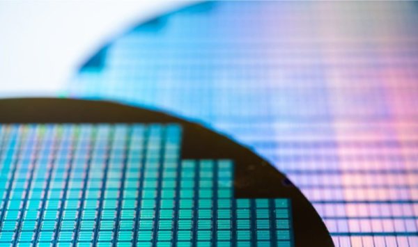
As NVIDIA is rushing to quickly increase GPU performance, the intermediary layer connecting memory and GPUs within the wafer will be converted from silicon to silicon carbide, which will be a new opportunity for Taiwan's silicon carbide industry.
In the past few months, the Silicon Carbide industry chain in Taiwan's semiconductor industry has increased rapidly, and the reason is related to NVIDIA.
In May this year, Wolfspeed, the global silicon carbide dragon, announced its bankruptcy, but in the same month, Xu Xiulan, chairman of Globe Crystal, said that Globe Crystal will jointly develop new silicon carbide products with customers. Not only the bulbous crystals in the silicon carbide market, Zhang Zhongjie, chairman of Geqi Compound Semiconductor Company, also revealed that the company is currently actively developing new products, and this product can be used in advanced semiconductor processes.
"Financial Information" interview learned that when the global silicon carbide supply chain fell into a cold winter due to China's major expansion, Taiwan's silicon carbide industry got a new opportunity due to NVIDIA's unending demand for GPU performance. Because in the blue picture of NVIDIA's new generation Rubin processor, in order to improve performance, the materials of the silicon intermediary layer are planned to be converted from silicon to silicon carbide.
If the IC made from CoWoS packaging is compared to a building and the NVIDIA GPU is compared to the factory in the building, the role of the silicon intermediary layer is like the floor board of the building. In addition to carrying the NVIDIA GPU, it can also connect the high-performance memory next to it, so that data can move quickly between the GPU and the memory. Currently, a GPU and multiple memory are configured in a silicon intermediary layer.
The base of this building is the original loading board. The space on the loading board is enough to put a few such "buildings", exchange the signal through the loading board, and finally package it into a chip.
Zhang Zhongjie revealed that the advanced semiconductor process is currently under study, and the silicon intermediary layer originally made of silicon is to be converted into silicon carbide, because the power consumption of future high-level chip plans is as high as 1,000 volts! In comparison, Tesla's fast charging voltage is only 350 volts.
Industry insiders have observed that NVIDIA is currently the company that most needs to adopt this technology, because NVIDIA's NVLink technology feature is that the closer the GPU and memory distance, the faster the transmission speed, the higher the power of the GPU, and the better the performance. In the future, NVIDIA even plans to tie the GPU and the memory together and drive with extremely large currents. Since the thermal conduction of silicon carbide is better than that of copper, it can effectively solve the high heat generated by large currents, it is favored by NVIDIA.
However, if silicon carbide is used as an intermediary layer, it requires different from traditional silicon carbide. Industry insiders analyzed that the crystal factory treats silicon carbide as an intermediary layer material. Therefore, the structural defects that traditional silicon carbide industry cares about have little impact on the manufacturing of intermediary layers, but the key is in the cutting technology, and the hardness of silicon carbide is comparable to diamonds. If the cutting technology is not good, the surface of silicon carbide will be wavy and cannot be used for advanced packaging.
In addition, the use of absolutely single crystal silicon carbide to make silicon intermediary layers has the best heat-guiding effect and must be as large as existing silicon wafers. Since most Chinese silicon carbide manufacturers can only manufacture 6-inch and 8-inch silicon carbide wafers at present, investing in the production of larger single crystal silicon carbide wafers has become the focus of the difference between Taiwanese manufacturers and Chinese competitors.
"Financial Information" quoted industry insiders as an investigation. Currently, Taiwan Electric has invited manufacturers from all over the world to jointly develop the manufacturing technology of silicon carbide intermediary layers, but cutting equipment manufacturers such as Japan DISCO are developing a new generation of laser cutting machines. Therefore, NVIDIA's Rubin The first generation of GPUs will still use silicon intermediary layers. When new equipment is in place, silicon carbide intermediary layers will be manufactured more smoothly. However, because NVIDIA has extremely high requirements for performance improvement, when the heat generated in the chip exceeds the limit, silicon carbide must be used. "At the latest year afterward, silicon carbide will enter advanced packaging."
Since this technology is currently only used on the cutting-edge AI chips, the Taiwan Supply Chain will be the first to use silicon carbide wafers outside of China. This technology will be a new opportunity for Taiwan's silicon carbide manufacturers.
Extended reading: Tokyo Direct Shot》Rosen took KDDI with smart technology to create a future convenience store and solve the problem of high-end and low-birth human resources Kim Jong-un and Putin attended the 9/3 China Soldiers. What information did the leaders of the "Strange Heart" gather together to convey to the Russian-UK war? Micron Taiwan-Japanese DRAM operator Ludongxing, the leader of Taiwan, has independently developed and transformed the cold factory for the first time


